I. Features
Functional thin films are deposited on circuit substrates such as alumina, aluminum nitride, beryllium oxide, ferrite, glass ceramic, quartz, diamond, and silicon carbide. Thin-film inductors, thin-film resistors, thin-film capacitors, microstrip lines, and other elements are integrated on the same circuit board to form thin-film circuits. The components offer a wide parameter range, high precision, good temperature and frequency characteristics, operation up to 100 GHz+, high integration, and small size. Products include thin-film circuits, circulators/isolators, ceramic support plates, shorting plates, heat sinks, microwave dielectric substrates, and AuSn preform pads.
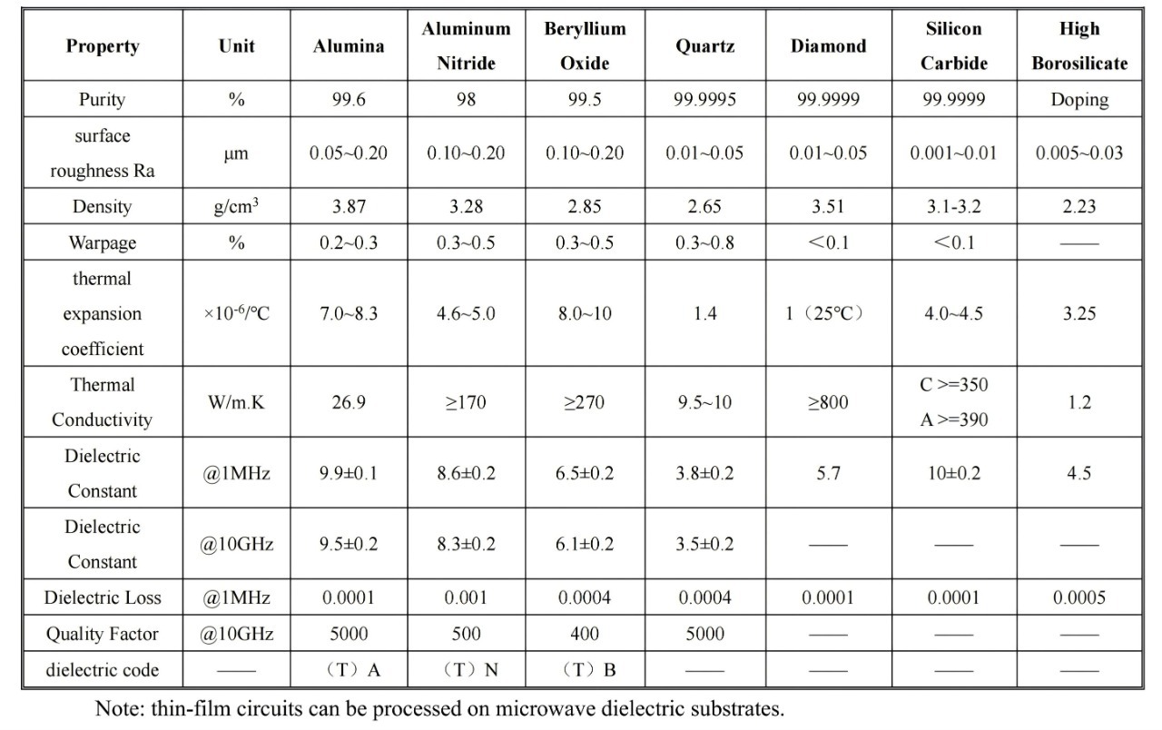
II. Substrates and Performance
Ⅲ:Normal Thickness and Codes

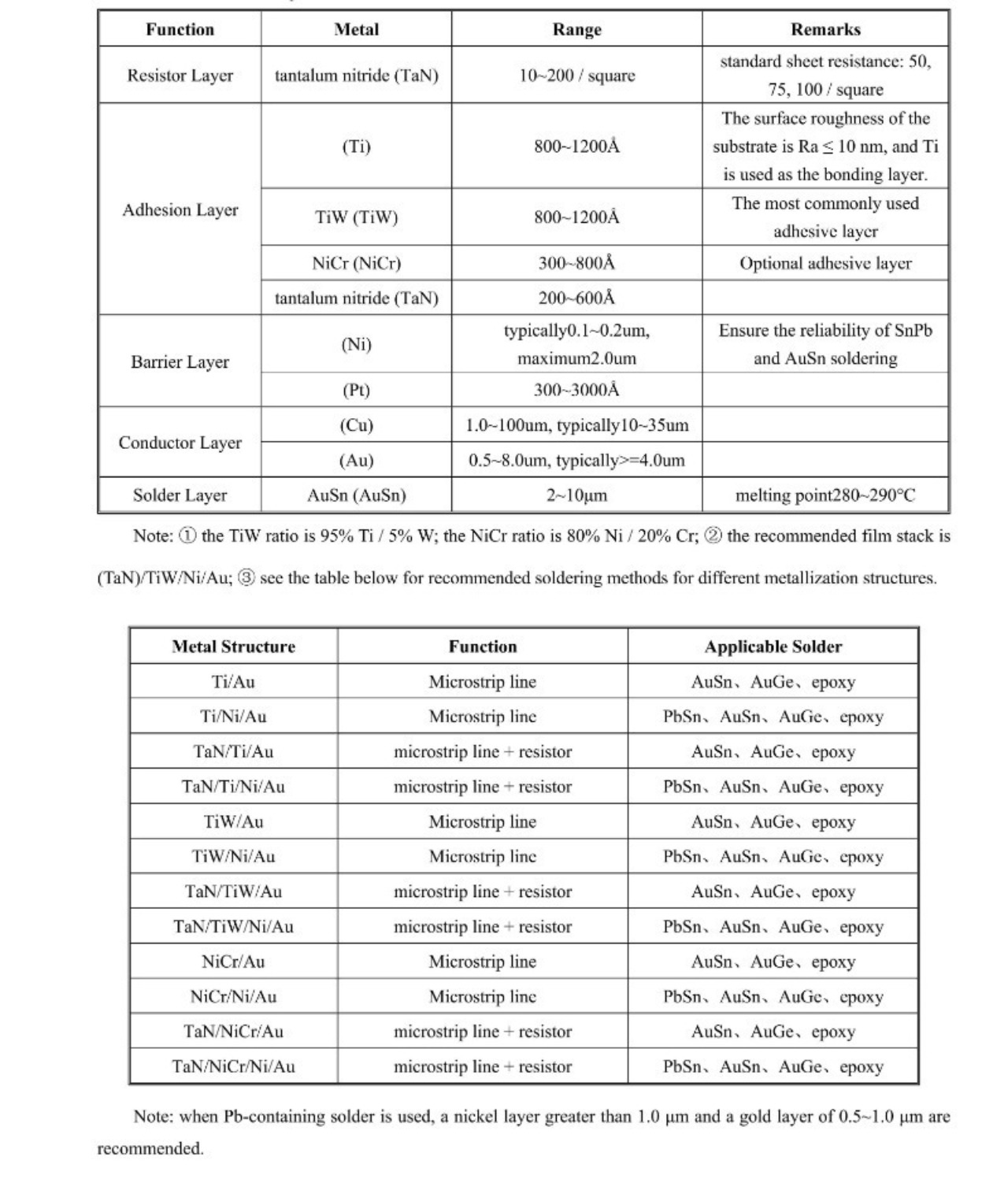
IV. Metallization System
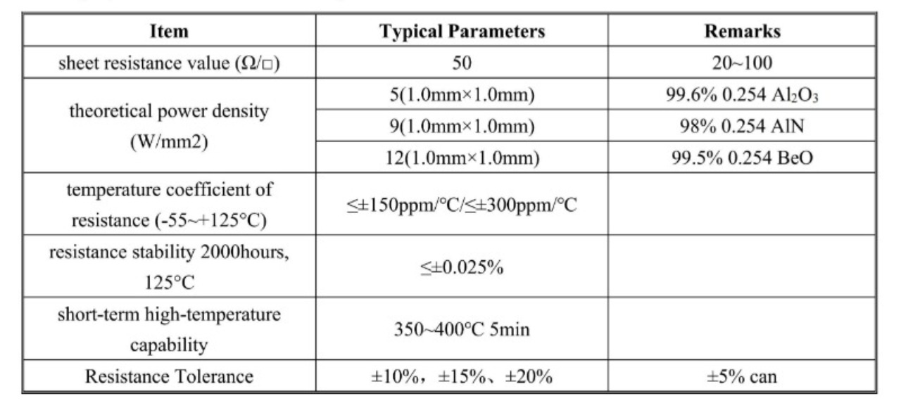
V. Thin-Film Resistors
The company's thin-film circuits can integrate thin-film resistors or thin-film resistor networks.
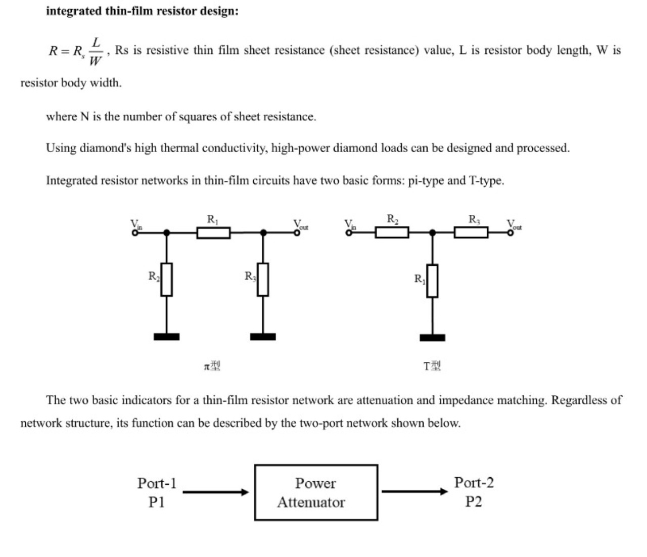
In the figure, the signal input power is P1 and the output power is P2. The attenuation of the resistor network is A (dB). If P1 and P2 are expressed in dBm, the relationship between the two powers is:
Attenuation describes how much power decreases after passing through the attenuator. The attenuation value is determined by the materials and structure of the attenuator. Attenuation is expressed in decibels, which facilitates system-level performance calculations.
Pi-type or T-type networks made from resistors implement lumped-parameter attenuation. In general, attenuation is fixed and determined by three resistor values. Z1 and Z2 usually denote the characteristic impedances at the circuit input and output. At the input, the input impedance should match the source output impedance; at the output, the output impedance should match the load impedance. Since resistor networks used for attenuation in RF power circuits do not require impedance transformation, the input impedance, output impedance, load impedance, and source output impedance are equal. Most equipment has a specified input impedance; for example, most communication equipment uses 50 ohms.
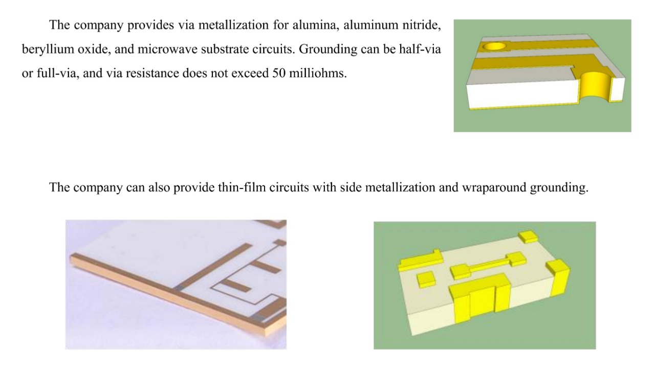
VI. Via / Sidewall Metallization
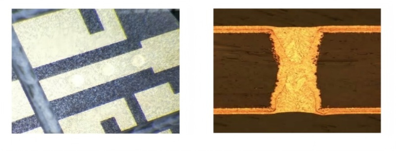
VII. Filled Vias
The company provides filled-via thin-film circuits on alumina and aluminum nitride. Via diameter is 0.08-0.15
mm, and the edge-to-edge spacing between adjacent vias is >=0.20 mm. Fill materials may include copper, silver, and
polyimide (PI).
VIII. Polyimide Dielectric Bridges
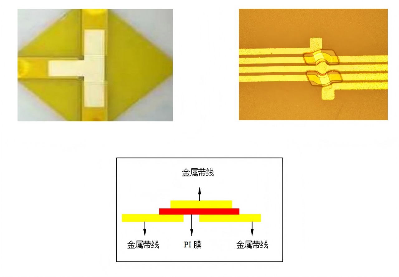
The company can provide polyimide (PI) dielectric bridges on thin-film circuit surfaces.
IX. Side Patterning
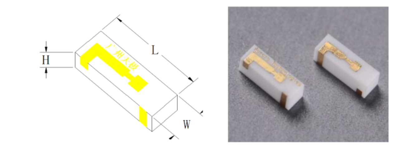
Note: Side patterning can only be used to process microstrip lines. The maximum width of side-patterned products
is 3.0 mm.
X. Solder Mask
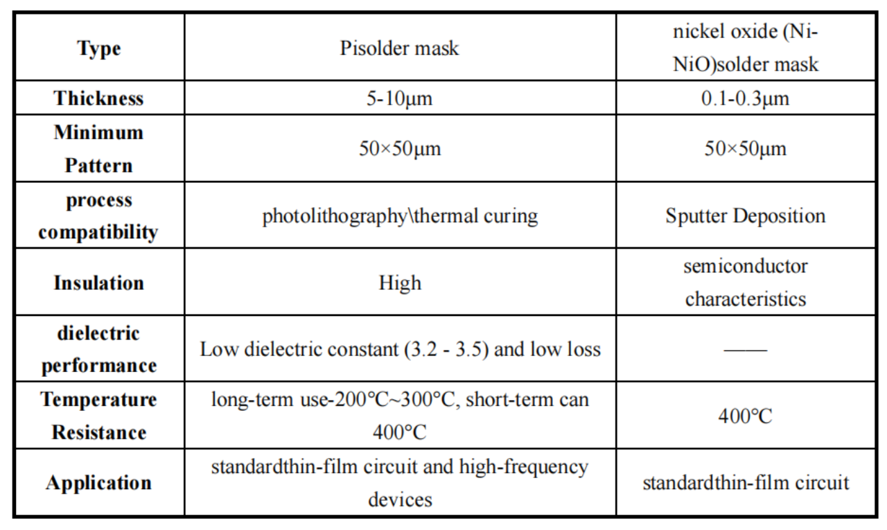
The surface or side of our products are coated with a solder mask layer. Currently, there are two types: nickel oxide (Ni-NiO) and PI solder mask..
XI. AuSn Preform Pads
◼ and AuSn solder preform, reduced thickness, low cost;
◼ AuSn: Au: Sn=70: 30~82: 18 (wt%);
◼ melting point: 280~290°C, soldering temperature 300~320°C;
◼ thickness: 2~10um;
◼ film-stack form: Ti/Pt/AuSn or Ti/Pt/AuSn/Au or TiW/Ni/Au/AuSn.
XII. Pattern Accuracy
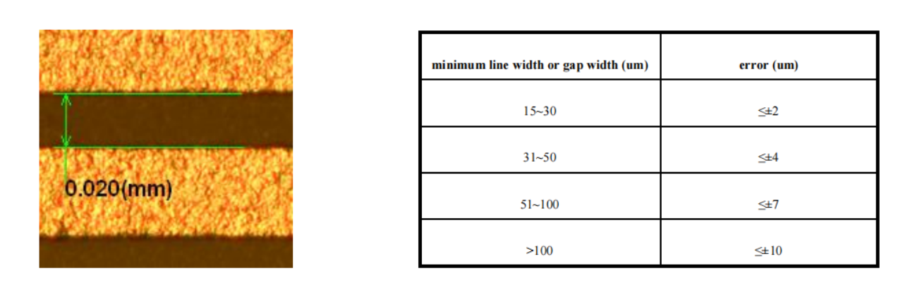
◼ minimum line width and gap width: front and back sides figure shape minimum line width and gap width is 15um, error<=±2um; side pattern minimum line width and gap width is 100um, error<=±10um.
◼ alignment error: front and back sidesalignment error<=±25um; same side overlay error<=±25um, front side and side alignment error<=±25um.
◼ line width, gap width tolerance
XIII. Outline and Tolerances
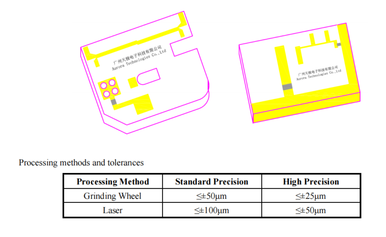
The company's thin-film circuits are usually rectangular, but non-rectangular circuits with chamfered or rounded corners are also available. Mounting holes can be processed inside the circuit. Rectangular areas are processed by dicing-saw cutting, while non-rectangular areas are processed by laser.
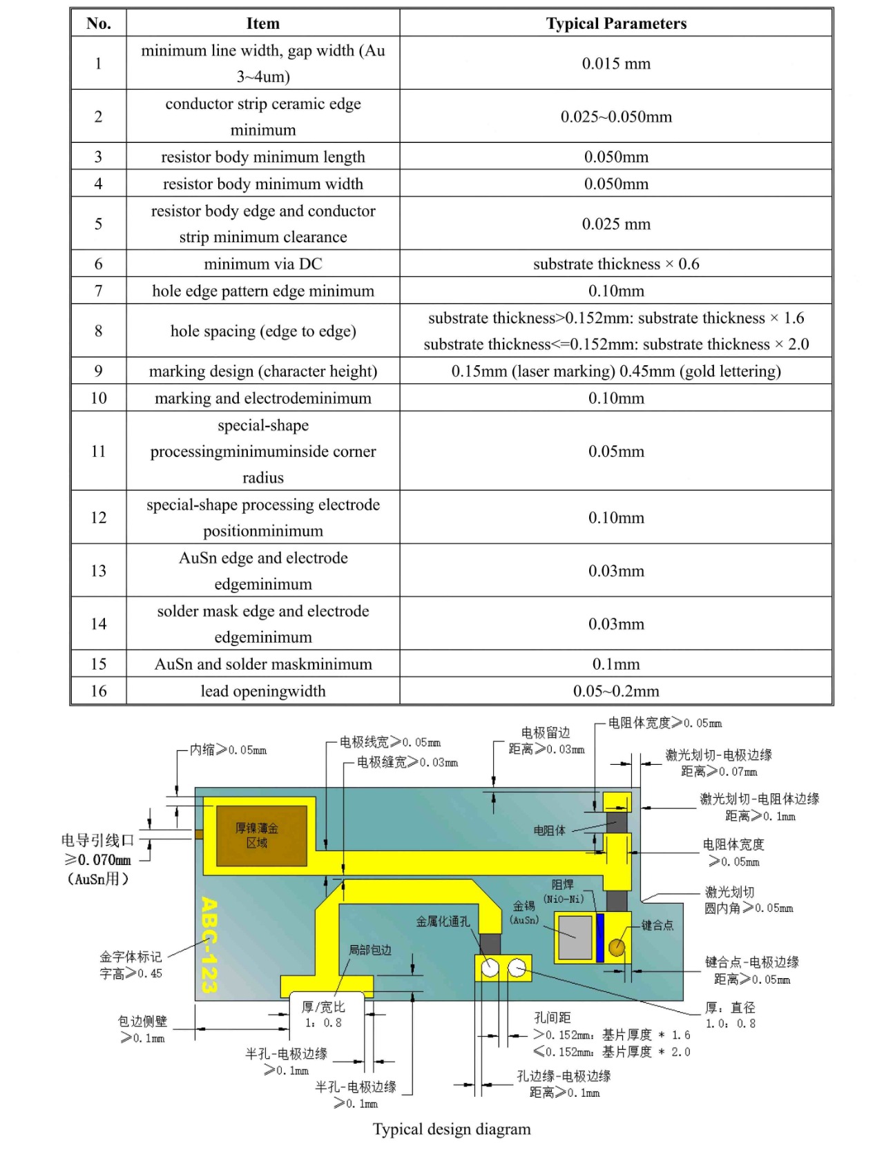
XIV. Thin-Film Circuit Design Rules




 Soporta red IPv6